This page is a companion page for my MSP430 Launchpad page.
1. SPI communications with ktm-s1201 LCD panel
I picked up a set of inexpensive 12 digit LCD panels ("new old stock" panels) on the web. Communication is via SPI (Serial Peripheral Interface), so I wired one up to an msp430g2211 and started studying data sheets. Since this microcontroller doesn’t have hardware serial support (and since I wanted to learn about how the protocol works) I decided to do a bit-banged serial program. To get things wired up, I used this (somewhat abreviated) data sheet: data/ktm-s1201.pdf
From the LCD panel, these connections are made:
-
Pin 1 Vcc — Vcc on the Launchpad (+3.3V)
-
Pin 2 Vss — GND on the Launchpad
-
Pin 3 SCK — P1.6 on the Launchpad (which I’ve used for the serial clock line)
-
Pin 4 SI — P1.0 on the Launchpad (which I’ve used for Master-out Slave-in line)
-
Pin 5 C/D — P1.7 on the Launchpad (which I’ve used for the Command/Data selector)
-
Pin 6 Reset — Needs to be pulled high. This can be done with a high-value resistor, like 10K, connected to Vcc.
-
Pin 7 Busy — Can be left disconnected as long, as you don’t drive the LCD too fast. Normally the panel uses this line to tell the microcontroller to wait.
-
Pin 8 CS — P1.5 on the Launchpad (which I’ve used for chip select)
-
Pin 9 Vlc — Described below
-
Pin 10 NC — Not connected
On the data sheet, Pin 9 is shown connected to the center pin of a variable resistor whose ends are connected to Vcc and GND. I used a 10K potentiometer that I had on hand. This arrangement effectively creates a voltage divider, with an adjustable intermediate voltage on the middle pin (connected to Pin 9). This is how you set the contrast of the LCD so you can actually see text on it.
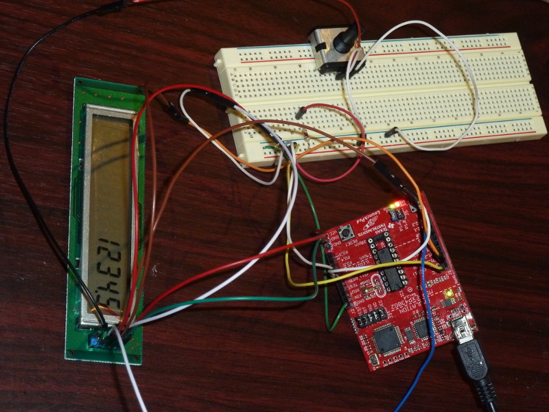
There’s nothing particularly important about the specific Launchpad pin assignments. When learning, I usually configure significant lines on the pins that have LEDs, so I can watch the lights and have an idea if things are working. That’s why I put the clock line on P1.6 (so the clock line shows on the green Launchpad LED) and the data line on P1.0 (so data shows on the red Launchpad LED). But they could all be changed with minimal changes to the code.
A somewhat minimal SPI bit-banging example program follows. The key function is spi_IO(), which handles the serial communication with the panel, effectively putting bits on the MOSI line one at a time and pulsing the clock pin. The other helper functions; init_lcd(), print_lcd(), and decimal_on(); all call this function.
#include <msp430g2211.h>

#define CS BIT5         // Chip Select line
#define CD BIT7         // Command/Data mode line
#define MOSI BIT0       // Master-out Slave-in
#define SCK BIT6        // Serial clock

#if 20110706 > __MSPGCC__
/* A crude delay function. */
void __delay_cycles( unsigned long n ) {
    volatile unsigned int i = n/6;
    while( i-- ) ;
}
#endif

/* Write data to slave device.  Since the LCD panel is
 * write-only, we don't worry about reading any bits.
 * Destroys the data array (normally received data would
 * go in its place). */
void spi_IO( unsigned char data[], int bytes ) {
    int i, n;

    // Set Chip Select low, so LCD panel knows we are talking to it.
    P1OUT &= ~CS;
    __delay_cycles( 500 );

    for( n = 0; n < bytes; n++ ) {
        for( i = 0; i < 8; i++ ) {
            // Put bits on the line, most significant bit first.
            if( data[n] & 0x80 ) {
                P1OUT |= MOSI;
            } else {
                P1OUT &= ~MOSI;
            }
            data[n] <<= 1;

            // Pulse the clock low and wait to send the bit.  According to
            // the data sheet, data is transferred on the rising edge.
            P1OUT &= ~SCK;
            __delay_cycles( 500 );

            // Send the clock back high and wait to set the next bit.  Normally
            // we'd also read the data bits here, but the LCD is write-only.
            P1OUT |= SCK;
            __delay_cycles( 500 );
        }
    }

    // Set Chip Select back high to finish the communication.
    // For data, this also triggers the LCD to update/display.
    P1OUT |= CS;
}

/* Sets the LCD to command mode, and sends a 7-byte
 * sequence to initialize the panel. */
void init_lcd( void ) {
    unsigned char data[] = {
        0x40, // M=0(4-share-1/3 duty; FF=0)
        0x30, // Unsynchronized transfers
        0x18, // Blink off
        0x11, // Display on
        0x15, // Segment Decoder ON
        0x20, // Clear Data and pointer
        0x00  // Clear blink memory
    };

    P1OUT |= CD;        // set for commands

    spi_IO( data, sizeof(data));
}

/* Prints a string on the LCD panel using the 7 segment decoder.
 * Understood characters are 0x00 (zero) to 0x09 (nine) and
 * 0x0A to 0x0F (the symbols -, E, C, =, and space). */
void print_lcd( unsigned char data[], int n ) {
    unsigned char copy[12];
    unsigned char tmp;
    int i;

    if( n < 1 ) return;
    if( n > 12 ) n=12;

    // The panel expects data arranged right to left, so we'll
    // reverse the array of data passed before writing it out.
    for( i = n; i > 0; i-- ) {
        copy[n-i] = data[i-1];
    }

    P1OUT &= ~CD;       // set for data

    spi_IO( copy, n );
}

/* Draws a decimal point n places from the right, by turning on
 * the individual LCD segment (OR 0x8 mask with segment memory). */
void decimal_on( int n ) {
    unsigned char data[] = {
        0x14,           // Segment Decoder off
        0xE0+2*n,       // Set pointer 0 (plus 2 for each digit)
        0xB8,           // Decimal point on (OR 0x8 with memory contents)
        0x15            // Segment Decoder on
    };

    if( n < 0 || n > 11 ) return;

    P1OUT |= CD;        // set for commands

    spi_IO( data, sizeof(data));
}

void main( void ) {
    // Stop the watchdog timer so it doesn't reset our chip
    WDTCTL = WDTPW + WDTHOLD;

    // These are the pins we need to drive.
    P1DIR |= SCK + MOSI + CS + CD;

    // De-select the LCD panel and set the clock high
    P1OUT |= CS + SCK;

    // Pause so everything has time to start up properly.
    __delay_cycles( 15000 );

    // Initialize the LCD panel.
    init_lcd();

    // Print a message: 1234.5
    print_lcd("\1\2\3\4\5", 5 );
    decimal_on( 1 );

    for( ;; ) {
        __bis_SR_register( LPM3_bits + GIE );
    }
}
The next program adds functions to take advantage of most all the features/commands offered by the LCD controller chip on the panel (an NEC uPD7225). Details are in the data sheet: data/upd7225.pdf This data sheet is also where I learned specifics of the serial protocol (that bits are written on the rising clock edge for example).
The decimal_off() function complements the decimal_on() function.
The write_segments() function can turn on arbitrary segments of the display, so symbols other than the stock 15 symbols may be displayed. For example capital A and lower case b could be displayed by turning on the correct individual segments.
The write_blinking() function is similar, but it marks segments on the display that (if also set in the segment memory) will blink on and off. The blink_on() and blink_off() modify the master flag that controls whether blinking happens. Finally, the display_on() and display_off() turn on and off the entire display.
#include <msp430g2211.h>

#define CS BIT5         // Chip Select line
#define CD BIT7         // Command/Data mode line
#define MOSI BIT0       // Master-out Slave-in
#define SCK BIT6        // Serial clock

#if 20110706 > __MSPGCC__
/* A crude delay function. */
void __delay_cycles( unsigned long n ) {
    volatile unsigned int i = n/6;
    while( i-- ) ;
}
#endif

/* Write data to slave device.  Since the LCD panel is
 * write-only, we don't worry about reading any bits.
 * Destroys the data array (normally received data would
 * go in its place). */
void spi_IO( unsigned char data[], int bytes ) {
    int i, n;

    // Set Chip Select low, so LCD panel knows we are talking to it.
    P1OUT &= ~CS;
    __delay_cycles( 500 );

    for( n = 0; n < bytes; n++ ) {
        for( i = 0; i < 8; i++ ) {
            // Put bits on the line, most significant bit first.
            if( data[n] & 0x80 ) {
                P1OUT |= MOSI;
            } else {
                P1OUT &= ~MOSI;
            }
            data[n] <<= 1;

            // Pulse the clock low and wait to send the bit.  According to
            // the data sheet, data is transferred on the rising edge.
            P1OUT &= ~SCK;
            __delay_cycles( 500 );

            // Send the clock back high and wait to set the next bit.  Normally
            // we'd also read the data bits here, but the LCD is write-only.
            P1OUT |= SCK;
            __delay_cycles( 500 );
        }
    }

    // Set Chip Select back high to finish the communication.
    // For data, this also triggers the LCD to update/display.
    P1OUT |= CS;
}

/* Sets the LCD to command mode, and sends a 7-byte
 * sequence to initialize the panel. */
void init_lcd( void ) {
    unsigned char data[] = {
        0x40, // M=0(4-share-1/3 duty; FF=0)
        0x30, // Unsynchronized transfers
        0x18, // Blink off
        0x11, // Display on
        0x15, // Segment Decoder ON
        0x20, // Clear Data and pointer
        0x00  // Clear blink memory
    };

    P1OUT |= CD;        // set for commands

    spi_IO( data, sizeof(data));
}

/* Prints a string on the LCD panel using the 7 segment decoder.
 * Understood characters are 0x00 (zero) to 0x09 (nine) and
 * 0x0A to 0x0F (the symbols -, E, C, =, and space). */
void print_lcd( unsigned char data[], int n ) {
    unsigned char copy[12];
    unsigned char tmp;
    int i;

    if( n < 1 ) return;
    if( n > 12 ) n=12;

    // The panel expects data arranged right to left, so we'll
    // reverse the array of data passed before writing it out.
    for( i = n; i > 0; i-- ) {
        copy[n-i] = data[i-1];
    }

    P1OUT &= ~CD;       // set for data

    spi_IO( copy, n );
}

/* Draws a decimal point n places from the right, by turning on
 * the individual LCD segment (OR 0x8 mask with segment memory). */
void decimal_on( int n ) {
    unsigned char data[] = {
        0x14,           // Segment Decoder off
        0xE0+2*n,       // Set pointer 0 (plus 2 for each digit)
        0xB8,           // Decimal point on (OR 0x8 with memory contents)
        0x15            // Segment Decoder on
    };

    if( n < 0 || n > 11 ) return;

    P1OUT |= CD;        // set for commands

    spi_IO( data, sizeof(data));
}

/* Erases a decimal point n places from the right, by turning off
 * the individual LCD segment (AND 0x7 mask with segment memory). */
void decimal_off( int n ) {
    unsigned char data[] = {
        0x14,           // Segment Decoder off
        0xE0+2*n,       // Set pointer 0 (plus 2 for each digit)
        0x97,           // Decimal point off (AND 0x7 with memory contents)
        0x15            // Segment Decoder on
    };

    if( n < 0 || n > 11 ) return;

    P1OUT |= CD;        // set for commands

    spi_IO( data, sizeof(data));
}

/* Writes a custom configuration of segments in the digit n places from
 * the right, by writing 8 bits directly to the segment memory.
 * Mask values:
 *  0x01 = top          0x10 = top-left
 *  0x02 = top-right    0x20 = middle
 *  0x04 = bottom-right 0x40 = bottom-left
 *  0x08 = decimal      0x80 = bottom      */
void write_segments( int n, unsigned char bits ) {
    unsigned char data[] = {
        0x14,           // Segment Decoder off
        0xE0+2*n,       // Set pointer 0 (plus 2 for each digit)
        0xD0+(bits&0xF),// Write contents (4 bits)
        0xD0+(bits>>4), // Write contents (4 bits)
        0x15            // Segment Decoder on
    };

    P1OUT |= CD;        // set for commands

    spi_IO( data, sizeof(data));
}

/* Blinks a custom configuration of segments in the digit n places from
 * the right, by writing 8 bits directly to the blink memory.  Segments
 * only blink if they are set, and if the blink state is set on.
 * Mask values:
 *  0x01 = top          0x10 = top-left
 *  0x02 = top-right    0x20 = middle
 *  0x04 = bottom-right 0x40 = bottom-left
 *  0x08 = decimal      0x80 = bottom      */
void write_blinking( int n, unsigned char bits ) {
    unsigned char data[] = {
        0x14,           // Segment Decoder off
        0xE0+2*n,       // Set pointer 0 (plus 2 for each digit)
        0xC0+(bits&0xF),// Write contents (4 bits)
        0xC0+(bits>>4), // Write contents (4 bits)
        0x15            // Segment Decoder on
    };

    P1OUT |= CD;        // set for commands

    spi_IO( data, sizeof(data));
}

/* Send the command to enable blinking.  (Only segments set in blink
 * memory actually blink, and only if they are on in segment memory.) */
void blink_on() {
    unsigned char cmd = 0x1A;

    P1OUT |= CD;        // set for commands

    spi_IO( &cmd, 1 );
}

/* Send the command to disable blinking. */
void blink_off() {
    unsigned char cmd = 0x18;

    P1OUT |= CD;        // set for commands

    spi_IO( &cmd, 1 );
}

/* Send the command to clear the blink memory. */
void clear_blinking() {
    unsigned char cmd = 0x00;

    P1OUT |= CD;        // set for commands

    spi_IO( &cmd, 1 );
}

/* Send the command to turn clear the display. */
void clear_lcd() {
    unsigned char cmd = 0x20;

    P1OUT |= CD;        // set for commands

    spi_IO( &cmd, 1 );
}

/* Send the command to turn off the display. */
void display_off() {
    unsigned char cmd = 0x10;

    P1OUT |= CD;        // set for commands

    spi_IO( &cmd, 1 );
}

/* Send the command to turn on the display. */
void display_on() {
    unsigned char cmd = 0x11;

    P1OUT |= CD;        // set for commands

    spi_IO( &cmd, 1 );
}

void main( void ) {
    // Stop the watchdog timer so it doesn't reset our chip
    WDTCTL = WDTPW + WDTHOLD;

    // These are the pins we need to drive.
    P1DIR |= SCK + MOSI + CS + CD;

    // De-select the LCD panel and set the clock high
    P1OUT |= CS + SCK;

    // Pause so everything has time to start up properly.
    __delay_cycles( 15000 );

    // Initialize the LCD panel.
    init_lcd();

    // Print a message.
    print_lcd("\x0A\x0B\x0C\x0D\x0F", 5 );

    clear_lcd();

    // Print 1234.5
    print_lcd("\1\2\3\4\5", 5 );
    decimal_on( 1 );

    for( ;; ) {
        __bis_SR_register( LPM3_bits + GIE );
    }
}
The commands for building and installing this program (using the msp430-gcc 4.5.3 compiler) are:
$ msp430-gcc -O2 -mmcu=msp430g2211 -o ktm-s1201.elf ktm-s1201.c
$ mspdebug rf2500 "prog ktm-s1201.elf"
2. SPI communications with EA DOGS102 LCD panel
I had so much fun learning SPI that I decided to attack another LCD panel I have on hand, an EA DOGS102. This is a 102x64 pixel graphical panel. The data sheet, data/dogs102-6e.pdf (page 4), is pretty clear about wiring up the display, which requires three 1uF capacitors for the voltage booster and a pull-up resistor (I used a 10k resistor) for the reset pin.
There are 4 more connections for the serial communication, and these are the hookups that correspond to the program that follows.
-
LCD pin 24 SDA — Launchpad P1.1
-
LCD pin 25 SCK — Launchpad P1.2
-
LCD pin 26 C/D — Launchpad P1.7
-
LCD pin 28 CS — Launchpad P1.5
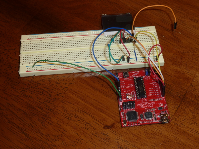
The dangling orange wire in the picture is hooked to the reset pin. If I need to reset the LCD, I can just touch it temporarily to ground.
The following code uses bit-banged SPI to initialize the panel and fill the LCD alternately with black, then white, then black, then white pixels. More info about the LCD controller is in the data sheet, data/uc1701.pdf.
#include <msp430g2211.h>

#define CS BIT5         // Chip Select line
#define CD BIT7         // Command/Data mode line
#define MOSI BIT1       // Master-out Slave-in
#define SCK BIT2        // Serial clock

#if 20110706 > __MSPGCC__
/* A crude delay function. */
void __delay_cycles( unsigned long int n ) {
    volatile unsigned int i = n/6;
    while( i-- ) ;
}
#endif

/* Write data to slave device.  Since the LCD panel is
 * write-only, we don't worry about reading any bits.
 * Destroys the data array (normally received data would
 * go in its place). */
void spi_IO( unsigned char data[], int bytes ) {
    int i, n;

    // Set Chip Select low, so LCD panel knows we are talking to it.
    P1OUT &= ~CS;
    __delay_cycles( 5 );

    for( n = 0; n < bytes; n++ ) {
        for( i = 0; i < 8; i++ ) {
            // Put bits on the line, most significant bit first.
            if( data[n] & 0x80 ) {
                P1OUT |= MOSI;
            } else {
                P1OUT &= ~MOSI;
            }
            data[n] <<= 1;

            // Pulse the clock low and wait to send the bit.  According to
            // the data sheet, data is transferred on the rising edge.
            P1OUT &= ~SCK;
            __delay_cycles( 5 );

            // Send the clock back high and wait to set the next bit.  Normally
            // we'd also read the data bits here, but the LCD is write-only.
            P1OUT |= SCK;
            __delay_cycles( 5 );
        }
    }

    // Set Chip Select back high to finish the communication.
    P1OUT |= CS;
}

/* Sets the LCD to command mode, and sends a 7-byte
 * sequence to initialize the panel. */
void init_lcd( void ) {
    unsigned char data[] = {
        0x40, // display start line 0
        0xA1, // SEG reverse
        0xC0, // Normal COM0-COM63
        0xA4, // Disable->Set All Pixel to ON
        0xA6, // Display inverse off
        0xA2, // Set Bias 1/9 (Duty 1/65)
        0x2F, // Booster, Regulator and Follower on
        0x27,
        0x81, // Set contrast
        0x10,
        0xFA, // Set temp compensation ...
        0x90, // ... curve to -0.11 %/degC
        0xAF  // Display On
    };

    P1OUT &= ~CD;       // set for commands

    spi_IO( data, sizeof(data));
}

/* Writes zeros to the contents of display RAM, effectively resetting
 * all of the pixels on the screen.  The screen width is 6*17 = 102 pixels,
 * so I used and array of size 17 and loop 6 times.  Each page in RAM
 * spans 8 pixels vertically, and looping through the 8 pages covers
 * the 8*8 = 64 pixel height of the display. */
void write_zeros( void ) {
    unsigned char zeros[17];
    int i, j, page;

    for( page = 0; page < 8; page++ ) {
        P1OUT &= ~CD;   // set for commands
        zeros[0] = 0xB0 + page; // set page
        zeros[1] = 0x00;        // LSB of column address is 0
        zeros[2] = 0x10;        // MSB of column address is 0
        spi_IO( zeros, 3 );

        P1OUT |= CD;    // set for data
        for( i = 0; i < 6; i++ ) {
            for( j = 0; j < 17; j++ ) zeros[j] = 0x00;

            spi_IO( zeros, sizeof( zeros ));
        }
    }
}

/* Writes ones to the contents of display RAM, effectively setting
 * all of the pixels on the screen.  The screen width is 6*17 = 102 pixels,
 * so I used and array of size 17 and loop 6 times.  Each page in RAM
 * spans 8 pixels vertically, and looping through the 8 pages covers
 * the 8*8 = 64 pixel height of the display. */
void write_ones( void ) {
    unsigned char ones[17];
    int i, j, page;

    for( page = 0; page < 8; page++ ) {
        P1OUT &= ~CD;   // set for commands
        ones[0] = 0xB0 + page;  // set page
        ones[1] = 0x00; // LSB of column address is 0
        ones[2] = 0x10; // MSB of column address is 0
        spi_IO( ones, 3 );

        P1OUT |= CD;    // set for data
        for( i = 0; i < 6; i++ ) {
            for( j = 0; j < 17; j++ ) ones[j] = 0xFF;

            spi_IO( ones, sizeof( ones ));
        }
    }
}

void main( void ) {
    // Stop the watchdog timer so it doesn't reset our chip
    WDTCTL = WDTPW + WDTHOLD;

    // These are the pins we need to drive.
    P1DIR |= SCK + MOSI + CS + CD;

    // De-select the LCD panel and set the clock high.
    P1OUT |= CS + SCK;

    // Pause so everything has time to start up properly.
    __delay_cycles( 5500 );

    // Initialize the LCD panel.
    init_lcd();

    // Blacken and clear the LCD two times.
    write_ones();
    write_zeros();
    write_ones();
    write_zeros();

    for( ;; ) {
        __bis_SR_register( LPM3_bits + GIE );
    }
}
The commands for building and installing this program (using the msp430-gcc 4.5.3 compiler) are:
$ msp430-gcc -O2 -mmcu=msp430g2211 -o dog-s102.elf dog-s102.c
$ mspdebug rf2500 "prog dog-s102.elf"
Maybe more experiments will follow. Since the DOGS102 doesn’t have a character generator, you’ll probably want to use a chip that has more than 2K of flash (i.e. the msp430g2211 wouldn’t be a great choice). You’ll need the space to hold something of a font.
A chip like the msp430g2553 would probably be better, if you intend to stick to through-hole DIP chips, and in that case you could also do much better than bit-banging the interface since you could use the USCI interface in the microcontroller. There are many capable chips if you don’t mind a harder soldering job or if surface mount is acceptable for you.
3. USI/SPI communications with EA DOGS102 LCD panel
Bit-banging SPI communication is pretty easy, but in general it’s not a great approach. In particular, blowing time in a wait loop tends to consume a lot more power than is really necessary. It would be much better to sleep and let one of the MSP430 clocks handle communication timing.
So I decided to rewrite my DOGS102 program to use the USI interface of the msp430g2231 chip (and similar). I had to give up on the msp430g2211 since it doesn’t have hardware serial support.
If I had planned ahead, I would have carried out my initial bit-bang experiments using the data and clock pins of the USI interface. But I didn’t so I had to re-wire my LCD panel to my Launchpad.
The new connections are:
-
LCD pin 24 SDA — Launchpad P1.6
-
LCD pin 25 SCK — Launchpad P1.5
-
LCD pin 26 C/D — Launchpad P1.2
-
LCD pin 28 CS — Launchpad P1.1
The primary changes to the program are:
-
In spi_IO(), instead of bit banging, we load bytes into the serial register and sleep while the data sends.
-
In the main() function, we set up the clocks and registers for the USI (universal serial interface).
-
There is a new interrupt handler USI_ISR(), which wakes up the main program after each byte has been transmitted.
#include <msp430g2231.h>
#include <legacymsp430.h>

/* For USI, these are the required pin assignments:
 * P1.5 SCLK -- serial clock
 * P1.6 SDO  -- serial data out (MOSI for master)
 * P1.7 SDI  -- serial data in (MISO for master) not connected
 *  in this program.
 * Chip Select line can be anything.
 * Command/Data line can be anything.  */

#define CS BIT1         // Chip Select line
#define CD BIT2         // Command/Data mode line

#if 20110706 > __MSPGCC__
/* A crude delay function. */
void __delay_cycles( unsigned long int n ) {
    volatile unsigned int i = n/6;
    while( i-- ) ;
}
#endif

/* Write data to slave device.  Since the LCD panel is
 * write-only, we don't worry about reading any bits.  */
void spi_IO( unsigned char data[], int bytes ) {
    int i, n;

    // Set Chip Select low, so LCD panel knows we are talking to it.
    P1OUT &= ~CS;

    for( n = 0; n < bytes; n++ ) {
        USISRL = data[n];       // load byte into USI serial register (lower half)
        USICNT = 8;             // set count to 8 bits
        __bis_SR_register( LPM0_bits + GIE );   // sleep until done
    }

    // Set Chip Select back high to finish the communication.
    P1OUT |= CS;
}

/* Sets the LCD to command mode, and sends a 7-byte
 * sequence to initialize the panel. */
void init_lcd( void ) {
    unsigned char data[] = {
        0x40, // display start line 0
        0xA1, // SEG reverse
        0xC0, // Normal COM0-COM63
        0xA4, // Disable->Set All Pixel to ON
        0xA6, // Display inverse off
        0xA2, // Set Bias 1/9 (Duty 1/65)
        0x2F, // Booster, Regulator and Follower on
        0x27, // Set...
        0x81, //  ...
        0x10, // ...contrast.
        0xFA, // Set temp compensation...
        0x90, // ...curve to -0.11 %/degC
        0xAF  // Display On
    };

    P1OUT &= ~CD;       // set for commands

    spi_IO( data, sizeof(data));
}

/* Writes zeros to the contents of display RAM, effectively resetting
 * all of the pixels on the screen.  The screen width is 6*17 = 102 pixels,
 * so I used and array of size 17 and loop 6 times.  Each page in RAM
 * spans 8 pixels vertically, and looping through the 8 pages covers
 * the 8*8 = 64 pixel height of the display. */
void write_zeros( void ) {
    unsigned char zeros[17];
    int i, j, page;

    for( page = 0; page < 8; page++ ) {
        P1OUT &= ~CD;   // set for commands
        zeros[0] = 0xB0 + page; // set page
        zeros[1] = 0x00;        // LSB of column address is 0
        zeros[2] = 0x10;        // MSB of column address is 0
        spi_IO( zeros, 3 );

        P1OUT |= CD;    // set for data
        for( i = 0; i < 6; i++ ) {
            for( j = 0; j < 17; j++ ) zeros[j] = 0x00;

            spi_IO( zeros, sizeof( zeros ));
        }
    }
}

/* Writes ones to the contents of display RAM, effectively setting
 * all of the pixels on the screen.  The screen width is 6*17 = 102 pixels,
 * so I used and array of size 17 and loop 6 times.  Each page in RAM
 * spans 8 pixels vertically, and looping through the 8 pages covers
 * the 8*8 = 64 pixel height of the display. */
void write_ones( void ) {
    unsigned char ones[17];
    int i, j, page;

    for( page = 0; page < 8; page++ ) {
        P1OUT &= ~CD;   // set for commands
        ones[0] = 0xB0 + page;  // set page
        ones[1] = 0x00; // LSB of column address is 0
        ones[2] = 0x10; // MSB of column address is 0
        spi_IO( ones, 3 );

        P1OUT |= CD;    // set for data
        for( i = 0; i < 6; i++ ) {
            for( j = 0; j < 17; j++ ) ones[j] = 0xFF;

            spi_IO( ones, sizeof( ones ));
        }
    }
}

void main( void ) {
    // Stop the watchdog timer so it doesn't reset our chip
    WDTCTL = WDTPW + WDTHOLD;

    // These are the pins we need to drive.
    P1DIR = CS + CD;

    // Pins to enable:
    //  P1.6 -- SDO/MOSI Master-out Slave-In
    //  P1.5 -- SCLK serial clock
    // Flags:
    //  most significant bit sent first
    //  enable output
    //  disable USI (for now)
    USICTL0 = USIPE6 | USIPE5 | USIMST | USIOE | USISWRST;

    // enable interrupts, but set the interrupt flag for now
    USICTL1 = USIIE | USIIFG;

    // Clock speed:
    //  Use clock divider 2^4=16.
    //  Use clock source 2 (submain clock?).
    // Polarity and phase settings/flags for the clock:
    //  SPI Mode 0 --- CPOL=0,CPHA=0  --- USICKPH
    //  SPI Mode 1 --- CPOL=0,CPHA=1  --- 0
    //  SPI Mode 2 --- CPOL=1,CPHA=0  --- USICKPL|USICKPH
    //  SPI Mode 3 --- CPOL=1,CPHA=1  --- USICKPL *** this one for DOGS panel
    USICKCTL = USIDIV_4 | USISSEL_2 | USICKPL;

    // enable USI
    USICTL0 &= ~USISWRST;

    // Clear the USI interrupt flag
    USICTL1 &= ~USIIFG;

    // Pause so everything has time to start up properly.
    __delay_cycles( 5500 );

    // Initialize the LCD panel.
    init_lcd();

    // Blacken and clear the LCD two times.
    write_ones();
    write_zeros();
    write_ones();
    write_zeros();

    for( ;; ) {
        __bis_SR_register( LPM3_bits + GIE );
    }
}

/* This interrupt triggers when the USI serial register gets
 * empty.  We use it to wake up the main program. */
interrupt(USI_VECTOR) USI_ISR(void) {
    USICTL1 &= ~USIIFG;         // clear the interrupt flag
    __bic_SR_register_on_exit( LPM0_bits );     // wake on exit
}
The commands for building and installing this program (using the msp430-gcc 4.5.3 compiler) are:
$ msp430-gcc -O2 -mmcu=msp430g2231 -o dog-s102-usi.elf dog-s102-usi.c
$ mspdebug rf2500 "prog dog-s102-usi.elf"